


Union Minister for Electronics and Information Technology Ashwini Vaishnaw on Friday, 6 November 2026, launched the Semicon 2.0 portal and announced 12 fresh approvals under the Electronics Components Manufacturing Scheme (ECMS). The Press Information Bureau, Ministry of Electronics and Information Technology said applications are now live for Pillars 2, 3 and 4 of Semicon 2.0, and that the 12 ECMS projects carry a projected investment of Rs 7,503 crore.
Those 12 projects are expected to generate production of Rs 39,045 crore and 7,127 direct jobs, according to the same release. The Hindu reported that the new tranche lifts total ECMS approvals to 118 applications and committed investment to Rs 77,051 crore.
Table of Contents
What the Semicon 2.0 portal opens
The Union Cabinet has approved Semicon 2.0 with a fiscal outlay of Rs 1,27,500 crore under the India Semiconductor Mission. The programme has six strategic pillars: design of chips; machines and materials; setting up more fabs; further strengthening the ATMP and OSAT industry; research and development; and talent development.
With Friday’s launch, applications are live for Pillar 2 (machines and materials), Pillar 3 (more fabs) and Pillar 4 (ATMP and OSAT). ETGovernment said Vaishnaw also framed Semicon 2.0 as a push for domestic capability in semiconductor equipment, materials, chemicals and gases, with a target of attracting at least three major equipment makers and five chemicals and gases firms to India.
The PIB note recalled that Semicon 1.0 had approved 12 projects across six states with cumulative investment of over Rs 1.64 lakh crore, and that five of those projects had begun commercial production as of October 2026.
What the 12 ECMS approvals cover
MeitY said the new approvals follow an earlier set of 106 applications involving investment of Rs 69,548 crore. The current 12 applications cover 10 target segment products across bare components, supply chain products and capital goods.
In components, multi layer PCB manufacturing was approved for NeST ICELR Private Limited; relays for TDConnex (Chennai) Private Limited; heat sinks for Modern Automotives Limited; and specialty ceramics for Voltix Semicon Private Limited.
On the supply chain side, Indo Asia Copper Limited received approval for copper foil; TACC Limited for anode material for lithium ion cells; Vidyuta Materials Private Limited for cathode active material; Enerfolie LLP for polypropylene film used in capacitor grade dielectric film; and Surface Modification Technologies Private Limited for camera rim.
Capital goods approvals went to TDConnex (Chennai) Private Limited for precision molds and tooling; Rockwell Automation India Private Limited for power and control systems for capital equipment; and Wipro Pari Robotics Private Limited for capital equipment for factory automation and system integration.
Where the projects will come up
The approved projects are spread across seven states: Gujarat, Karnataka, Madhya Pradesh, Maharashtra, Punjab, Tamil Nadu and Uttar Pradesh. The Hindu said Tamil Nadu accounts for four of the 12 projects, Gujarat and Maharashtra two each, and Punjab, Uttar Pradesh, Madhya Pradesh and Karnataka one each.
The same report identified the largest single commitment in the new tranche as a Rs 3,546 crore copper foil facility by Indo Asia Copper Limited in Amreli, Gujarat. The PIB said first time ECMS approvals in this round cover copper foil, cathode active material and specialty ceramics.
Incentives under ECMS are turnover linked, The Hindu noted, with government support tied to companies starting production. Overall ECMS numbers after this round, as stated by PIB, are 118 applications covering 34 products across 16 states, expected investment of Rs 77,051 crore, projected production of Rs 5,73,146 crore and direct employment for 81,755 persons.
What Vaishnaw told industry
Addressing the gathering, Vaishnaw said India’s electronics manufacturing has moved beyond assembly toward a fuller domestic value chain of modules, components, materials and advanced technologies. He pointed to growing work in battery cells, copper foils, copper clad laminates and high end printed circuit boards, and said nearly half the units approved under the scheme belong to the MSME sector.
ETGovernment quoted him saying the portal and the schemes are meant for serious, technologically capable players, not placeholders or frivolous applicants. The PIB release summarised his line that quality, technological depth, research and global competitiveness must guide semiconductor ambitions under Atmanirbhar Bharat.
That push to build industrial depth at home also runs through our earlier coverage of National Technology Day on 11 May and the broader story of modern industrial policy, including the draft National Steel Policy 2047.
Why the portal and the ECMS tranche matter together
Opening Semicon 2.0 applications for fabs, materials and packaging while clearing another ECMS batch is meant to thicken both the chip and the component layers of the same electronics stack. Copper foil, anode and cathode materials and specialty ceramics sit upstream of devices and batteries; multi layer PCBs, relays and heat sinks sit closer to finished electronics.
The Ministry’s own tally now puts ECMS well above its original investment target of Rs 59,350 crore that The Hindu cited. Whether every approved applicant reaches production will decide how much of the projected Rs 39,045 crore output and 7,127 jobs from this tranche actually arrives.
Friday’s announcement also sits in a longer national manufacturing story that readers can place against our explainer on Independence Day of India on 15 August, which tracks how industrial self reliance has been framed over decades.
For now, the verified facts are the portal launch for Pillars 2, 3 and 4; the Rs 1,27,500 crore Semicon 2.0 outlay; the 12 ECMS approvals at Rs 7,503 crore investment; and the cumulative ECMS scoreboard of 118 applications, Rs 77,051 crore investment and 81,755 expected direct jobs.
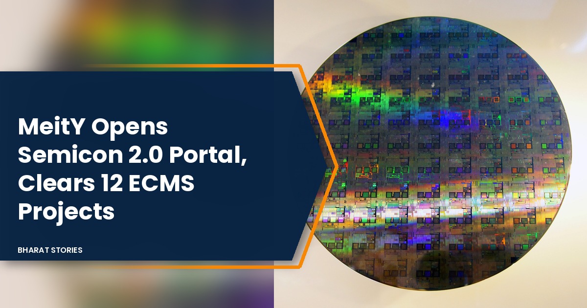
Featured image photo: Peellden, CC BY SA 3.0, via Wikimedia Commons. It shows a 12 inch silicon wafer and is used here to illustrate semiconductor manufacturing. Attribution is required under the Creative Commons licence.
FAQ
When was the Semicon 2.0 portal launched?
On 6 November 2026, by Union Minister Ashwini Vaishnaw, with applications live for Pillars 2, 3 and 4.
How large is the new ECMS tranche?
Twelve applications with projected investment of Rs 7,503 crore, production of Rs 39,045 crore and 7,127 direct jobs, according to the PIB release.
Sources
- Press Information Bureau, MeitY, 6 November 2026 (PRID 2333716): Semicon 2.0 portal launch; Pillars 2, 3 and 4; outlay Rs 1,27,500 crore; 12 ECMS approvals Rs 7,503 crore; production Rs 39,045 crore; 7,127 jobs; company and product list; cumulative 118 applications.
- The Hindu, 6 November 2026: total ECMS investment Rs 77,051 crore; Indo Asia Copper foil Rs 3,546 crore in Amreli; state wise project count; turnover linked incentives.
- ETGovernment, 6 November 2026: Vaishnaw on serious applicants; equipment and chemicals targets; Semicon 2.0 pillar framing.